Tall SU-8 Micropillars
If you’ve ever worked on microfabrication you’ve almost certainly come across SU-8. This polymer has a TON of uses across fields requiring microscale manufacturing. While my current postdoc work involves simple SU-8 processing protocols, much of my PhD work in microfluidics required some incredibly difficult designs. Most notably, I needed to fabricate high-density, 100um tall pillar arrays with up to 10:1 aspect ratios (height:width). This is no easy feat! For anyone who has worked with tall SU-8 pillar arrays, you know that many factors influence the fabrication process. Bake times, spin heights, exposure settings, and small tweaks to your design can all make or break the final device. Of course, all over the literature you’ll find Methods sections with some type of sentence “conventional photolithography techniques were used…” But let’s be real, that’s not helpful to anyone. In this post, you’ll find everything you need to know to fabricate 100um tall SU-8 structures with a 10um pitch. (PS: these devices were for worm microfluidics…see the end of the post for an immobilized C. elegans!)
I just spent the last hour laughing at my early grad school notes. So much frustration as I learned the ropes of fabrication! I had adhesion issues, pillars popping off, and pillars sticking together. I tried everything to fix it. Eventually, I was routinely able to fabricate 100um tall pillars with 10um spacing between pillars. The trick really came down to a long, low-temperature extra bake before exposure (in addition to some other important steps, detailed below). I stumbled across this method by accident. I was tweaking every step of the process. The prebake. The exposure. The postbake. The cleanliness of the wafer. Result after result not only failed but were also completely inconsistent, until I made a very small observation (through the use of thorough note taking, by the way!). My best looking devices all had large gaps of time between the prebake and exposure. I would routinely spin and bake many wafers, store them in a dark drawer, then expose them when necessary. For some reason, it looked like days of sitting in a drawer was directly correlated with a higher quality final device. From there, I realized I could replicate this long wait time with an extra low-temperature bake step.
Keeping with the philosophy of this blog, below is a step-by-step practical guide for each step in the protocol to fabricating 100um tall SU-8 micropillars.
Clean the wafer. Sonicate your silicon substrate (4” is what I used) in acetone for 5min. Rinse in IPA. Oxygen plasma clean for 5min. (Specifics of the plasma clean will vary depending on the tool you use. Note: the plasma cleaning step is significantly more important than the acetone clean in my experience).
Spin. SU-8 2050 to ~100um:
500rpm - 100rpm/s ramp - 10s
1750rpm - 300rpm/s ramp - 30s
Pre-bake. This is a multi-step bake. Also note that the bake times are significantly longer than what is suggested in the SU-8 processing manual. In general, my experience with thick SU-8 (>50um) is that the suggested bake times are too short.
5min - 65C
20min - 95C
Edge bead removal. This is critical for achieving tightly spaced, tall structures! For thick SU-8, the edge bead can be dozens of microns tall and will prevent a tight photomask-substrate contact during exposure. If you don’t remove the edge bead, you’re essentially performing the exposure with a significant gap between the photomask and your sample. For the spinner I used, I was able to very slowly spin the wafer with the spinner lid open. I then soaked the tip of a cleanroom wipe in acetone and placed it along the edge of the wafer. As the wafer spun, the edge bead was reduced evenly. I usually had to repeat the process with 2-3 cleanroom wipes. An alternative technique is to set the wafer on a flat surface during instead of using the spinner.
Extra bake. This is the secret sauce for achieving tall SU-8 with minimal cracking and straight walls. This bake serves two purposes: 1) Reduce the stickiness of the edge bead to avoid your wafer badly to the photomask during exposure. 2) Enable straight walls. I have no idea of the mechanism here. Driving off more solvents? Reducing stress on the SU-8? All I know is it works like a charm.
1min - 95C (Edge bead should be significantly less sticky)
20min - 60C (This low-temp bake is super important)
Exposure. I use an exposure dose of 530 mJ/cm^2 and hard contact. You’ll notice this is significantly larger than the recommended exposure. That’s because to attain straight walls, the exposure must be performed with UV wavelengths ~360nm or slightly greater. If your mask aligner is has a broadband source, I strongly suggest purchasing an additional glass filter to remove wavelengths <350nm (which will then increase the required exposure dose). Otherwise, the sidewalls will slant inwardly. If you’re making high-aspect ratio structures, slanted walls will lead to instability and likely cause these components to fall off the wafer. This effect is called “T-Topping” and you can read more about it here. An additional note: I always used glass/chrome photomasks for my SU-8 designs that required any type of fine structures. A lot of people prefer transparency masks because of their low-cost, but I was never able to get the same quality. The exposure can dramatically change as well. I only use transparencies for very simple structures with a height <50um.
Postbake.
5min - 65C
18min - 95C
Develop. In SU-8 developer, this is usually between 15-20min.
Hardbake. 1h - 200C. This reduces stress across the SU-8 and also significantly reduces microcracking that appears after developing. Be sure not to heat shock the wafer. Best practice is to place on a hot plate at room temp, then turn the plate to 200C. Likewise, after 1hr of baking, turn off the hotplate and do not remove the wafer until it has cooled to ~65C.
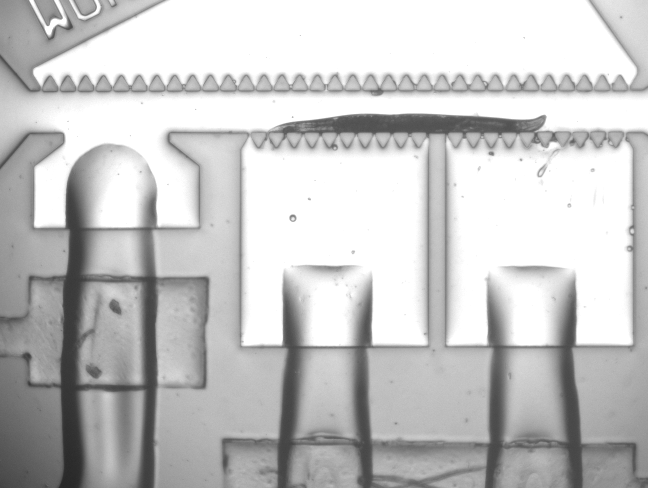
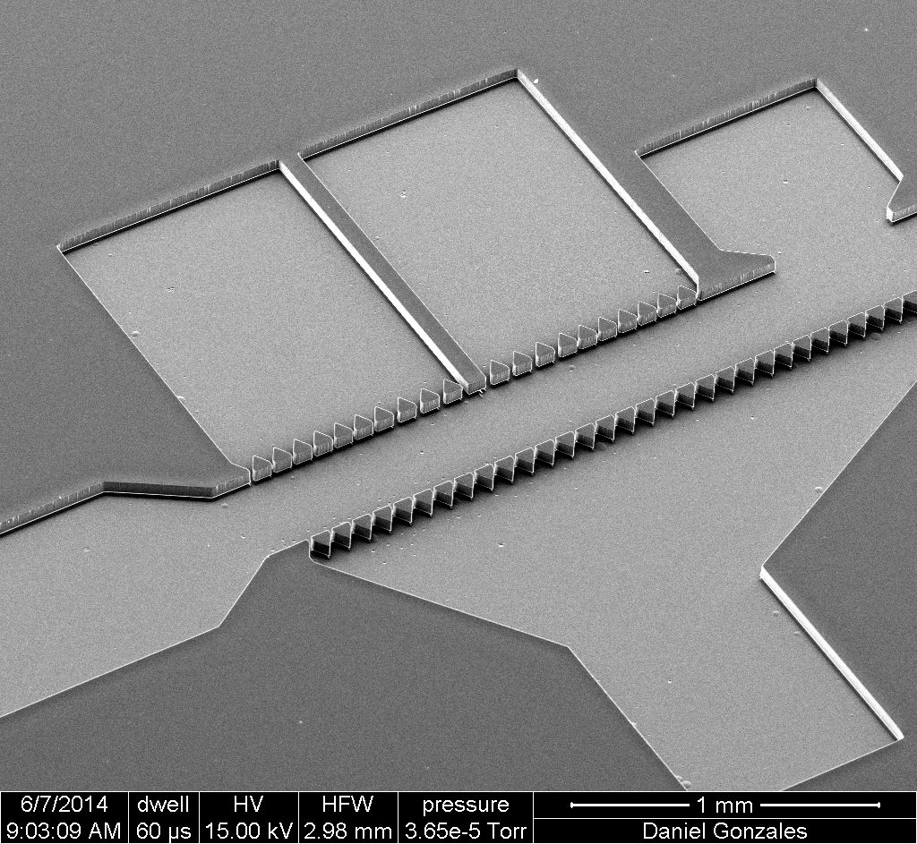
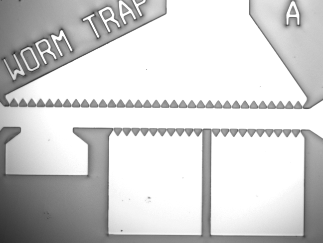
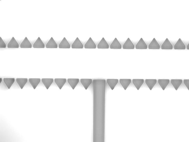
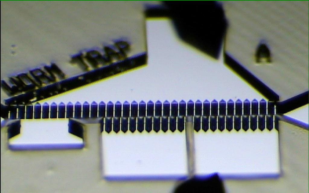
And that does it. Here are some pics of the final device. Nice straight walls. 10um between pillars. No peeling. Pillars perfectly stable. Perfect for worm microfluidics.
Also check out that SEM…can anyone spot the suspended nanowire? This process was the prelude to my first grad school publication involving suspended nanowires in microfluidic channels.